Technical Resource Home
Welcome to the LXD technical resources. Feel free to browse the many pages. If you have any questions about a current project, please contact us!
Application Notes
- Basic Operation of an LCD
- LCD Direct Drive Techniques
- Multiplexing LCD's
- Multiplexed Liquid Crystal Displays
- LCD Direct Drive Circuit
- Sample Multiplex Drive Circuit
- Temperature Compensation (With Schematic)
- Ghosting in LCD's
- Long Life / High Reliability LCD's
- LVDS Signal System for TFT Displays
- Glossary of Terms
- Active Matrix LCD
- Individual pixels of the display are controlled by thin film transistors, which are deposited directly onto the glass substrate. Each pixel is therefore driven in a static mode, resulting in very high contrast and viewing angle.
- Annunciator
- A word or special symbol which is driven as a single segment
- Array Process
- Method of manufacturing where displays are arranged in rows and columns on a large laminate and separated after they are filled with LCD fluid.
- Backplane
- The common electrode connection. There can be multiple backplanes in a multiplexed display.
- Common Plane
- Same as Backplane.
- Contact Ledge
- The area along the edge of the parts where electrical connections are made.
- Contrast Ratio
- The ratio of the luminance between the dark and light areas of the display.
- Dual in Line Pins (DIL)
- Two rows of pins attached along parallel sides of a display.
- Direct Drive
- A method of driving a display whereby individual segments are driven from separate edge connections.
- Elastomeric Connectors
- A thin conductive material used to make connections between an LCD and a PC board.
- First Minimum
- An LCD construction technique where the cell geometry is optimized for maximum contrast and viewing angle. The geometry is different for each LCD fluid.
- Font
- The style of a letter or digit.
- Ghosting
- A condition where segments which are in the "off" condition become slightly visible.
- Heat Seal Connector
- A thin flexible cable used to connect the LCD to the PC board.
- Image Area
- The total area bounded by the display characters.
- Ink Overlay
- The process of applying opaque, colored inks to the display to provide colors or highlight certain areas of annunciators.
- Isocontrast Plot
- Usually a polar plot showing contrast ratio versus viewing angle. The individual curves represent points of equal contrast.
- Liquid Crystal Flui
- An organic material which has both liquid and crystalline properties.
- Module
- An LCD which includes a PCB, driver electronics, bezel, and possibly, a backlight.
- Multiplex (Mux)
- A method of driving a display where multiple segments are driven from the same edge connection.
- Negative Image
- A display which has a dark background and lighter active segments, i.e. clear characters on a black background.
- Pixel
- An individual active segment.
- Polarizer
- A stretched polymer which transmits light in only one axis. A typical display has polarizers on the front and back.
- Positive Image
- A display which has a light background and darker active segments, i.e. black characters on a silver background.
- Reflective
- A viewing mode which uses ambient or other front lighting to provide the illumination for the display.
- Segment
- An active area within the display which can be turned on and off. This can be a single segment of a 7-segment character, an annunciator, or a pixel in a dot matrix array.
- Static Drive
- See Direct Drive
- Supertwist (STN)
- A type of display which uses fluids which "twist" greater than 90o. An STN display has improved viewing angles and contrast at high multiplex rates.
- Transflective
- A viewing mode which can use ambient light or backlighting to provide the illumination for the display.
- Transmissive
- A viewing mode which cannot use any type of front lighting to provide the illumination for the display, it therefore must use a backlight.
- Twisted Nematic (TN)
- A type of display where the liquid crystal fluid rotates the plane of polarization 90o.
- Viewing Area
- The area of a display which is visible through a bezel or cut-out in an instrument.
- Viewing Angle
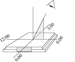
- The preferred angle of viewing a display, usually described in comparison to a clock face, i.e. 12 o'clock for above the normal, or 6 o'clock for below the normal.
- Parallel Interface
- Serial Interface
- Serial or Parallel Configuration to Microprocessor
- TFT Interface Examples
- Parallel Interface
- 16 Bit Data - Not Common - used on some graphic controllers
- 8 Bit Data - Most Common - used on graphic and character controllers
- 4 Bit Data - Used on some monochrome QVGA modules. An option on character controllers
- 8080 type - Parallel Data with Write Line, Read Line
- 6800 type - Parallel Data, with Read/Write Line, Enable Line
- Serial Interface
- Custom - Various configurations - Add Latch, Chip Select
- SPI (3 wire) uses Serial Data Out, Serial Data In, and Serial Clock
- SPI (4 wire) adds Chip Select
- Custom - Various configurations - Serial Data, Serial Clock, Latch, Chip Select
- Serial or Parallel Configuration to Microprocessor
- TFT Interface Examples
- What is a Liquid Crystal Display?
- What is Liquid Crystal Fluid?
- What is a Polarizer?
- What determines the Temperature Range?
- What is the Difference Between Reflective and Transflective?
- What is an Elastomer? A Heat Seal? A Pin?
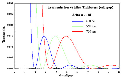
- What is "First Minima"?
- What is the Difference Between TN and STN?
- What is Direct Drive? Multiplexing?
- What is Viewing Mode?
- What is Contrast?
- What is Ghosting?
- What is Response Time?
- What is an Icon? Descriptor? Annunciator?
- How do you add Color to an LCD?
- How do you Backlight an LCD?
- What does "Ohms per Square" mean?
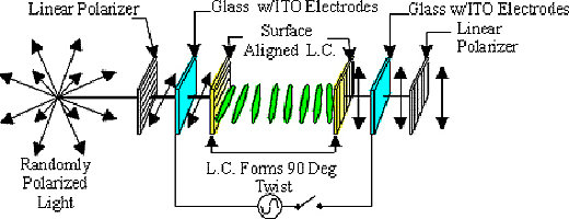
A liquid crystal display consists of two substrates that form a "flat bottle" that contains the liquid crystal mixture. The inside surfaces of the bottle or cell are coated with a polymer that is buffed to align the molecules of liquid crystal. The liquid crystal molecules align on the surfaces in the direction of the buffing. For twisted nematic devices, the two surfaces are buffed orthogonal to one another, forming a 90º twist of the liquid crystal from one surface to the other. See FIGURE 1.
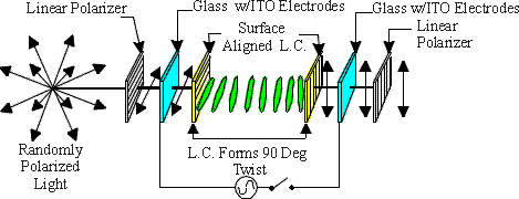
FIGURE 1
This helical structure has the ability to control light. A polarizer is applied to the front and an analyzer/reflector is applied to the back of the cell. When randomly polarized light passes through the front polarizer, it becomes linearly polarized. It then passes through the front glass and is rotated by the liquid crystal molecules and passes through the rear glass. If the analyzer is rotated 90º to the polarizer, the light will pass through the analyzer and be reflected back through the cell. The observer will see the background of the display, which in this case, is the silver-gray of the reflector.
When an appropriate drive signal is applied to the cell electrodes, an electric field is set up across the cell. The liquid crystal molecules will re-align with the electric field perpendicularly to the glass surface. The incoming linearly polarized light passes through the cell unaffected and is absorbed by the rear analyzer. The observer sees a black character on a sliver-gray background. See FIGURE 2. When the electric field is turned off, the molecules relax back to their 90º twist structure. This is referred to as a Positive Image, Reflective Viewing Mode.
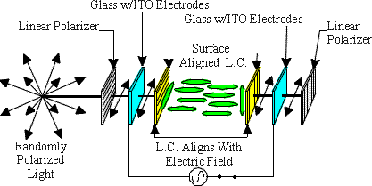
FIGURE 2
LCD's require an AC drive voltage with minimal DC component. Prolonged DC operation may cause electrochemical reactions inside the displays which will cause significantly reduced life. The initial indications of display degradation because of excessive DC current is an electro-plating of liquid crystal components onto the surface electrodes. These will appear as a mirror-like "burn-in" of the electrode pattern that was energized with DC. Elevated temperature will accelerate this effect.
Because an LCD is made up of several dielectric layers, the Equivalent Circuit shown below is a series of capacitors and a shunted resistor.
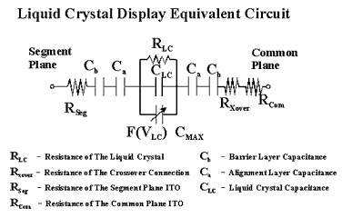
There are also series resistances to consider, including the resistivity of the indium oxide electrode paths and the crossover resistance. When voltages are specified for LCD operation, they refer to RMS (Root-Mean-Square) voltage, measured across the glass. For a static drive LCD, this is from an energized pin to the common plane.
Drive frequencies for direct drive displays are typically between 60Hz and 150Hz. Depending on the display size and design, displays can be operated at higher frequencies, but this will result in increased power consumption. Operation below 60Hz may result in display flicker. Electroplating may also occur at low frequencies when the speed of response of the liquid crystal is faster than the drive frequency. The net voltage that the liquid crystal would see would then have a DC component with respect to the speed of the fluid.
LCD's can be overdriven by a combination of voltage and frequency, which will result in cross talk or "ghosting" Ghosting is the appearance or partial activation of an "off" segment. At a specified viewing direction, the liquid crystal is formulated to begin turning on at a specific voltage, which is designated as the voltage threshold. By convention, this is the 10% on-state, or the condition where the contrast is 10% of the full-on contrast. Ghosting occurs when the effective RMS voltage across the display exceeds the voltage threshold of the liquid crystal.
On large displays with specific geometric designs, the backplane impedance could become a significant issue, where the voltage and current are out of phase. High drive voltage and/or frequency can contribute to produce voltages across segments that are at or above the voltage threshold. This will cause ghosting. This ghosting will always occur first at the off-axis condition called out as the optimum viewing angle. Since the current is directly proportional to the frequency, there is a voltage-frequency product which must not be exceeded. These values are very dependent on the design and layout of any given part, so proper display design and choice of driving conditions are important. It is also very important that all unused segments be connected to the backplane, and not allowed to float.
An actual drive circuit will be a symmetrical square wave with less than 50mV DC offset. The low DC offset drive circuit is best designed using a CMOS "exclusive OR" gate. Refer to the bottom part of the figure below:
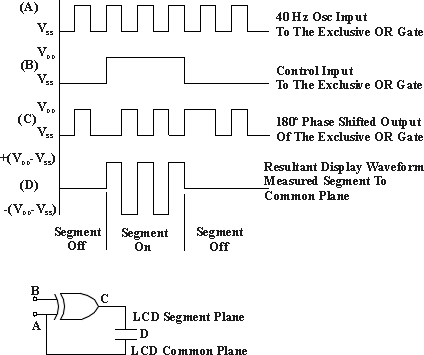
Please note that normal TTL devices are not suitable for drivers, as they typically have enough DC offset in their output signal to destroy an LCD. Today's commercially available display drivers are designed to produce the optimum signal output.
The top part of the above figure shows the output waveforms of our "exclusive OR" circuit. Plot A is the 40 Hz, 50% duty cycle square wave input to the XOR gate, or "clock" signal. Plot B is the control signal waveform which will turn a segment "on". Plot C is the output of the XOR gate. Plot D shows the RMS voltage as seen by the LCD segment.
Note that when the control input (B) is at logic 0, the resultant output signal to the segment is in phase with the clock output, resulting in a 0V RMS voltage at the segment. It will therefore remain in the "off" state. When the control input to the XOR goes high, the output shifts 180o out of phase to the backplane, resulting in an RMS value at the segment equal to the supply voltage. The segment will turn "on".
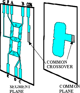
The drawing below shows a typical segment plane and common plane layout for a seven segment digit. From the drawing, it can be seen that the common plane electrode is made as large as possible to keep the resistance low and thereby eliminate "ghosting".
The details of designing a drive circuit for a multiplexed LCD are covered in our App note Multiplexed Liquid Crystal Displays. We will only cover the highlights here. We also have a sample drive circuit on in our Application Notes section, entitled A Sample Multiplex Drive Circuit. There are also numerous design guides available from the many LSI chip vendors, which contain excellent design tips and guidelines.
To aid in explaining the relationship between duty cycle and bias levels, we will choose a multiplex level of 64, which is a common multiplex duty cycle for a graphics display. To understand why specific bias levels are chosen, we will look at possible bias levels, and demonstrate why there is an optimum bias. What effect on the viewed display will switching between an LCD Bias of 1/9 and 1/8 have? Why is LCD Bias limited to 1/9 and 1/8 for Duty = 64?
The duty cycle defines the recommended bias. There are optimum bias levels for each duty cycle that will define the largest on/off voltage ratio to the LCD. The following formulas define the on and off voltages that the display will see for a given mux level and bias configuration.
Vrms OFF = Vb ⁄ S [((N-1) + (S-2)2)/N]1/2 where Vb is the bias (supply) voltage
Vrms ON = Vb ⁄ S [((N-1) + S2)/N]1/2
S = bias => 1 + √N (nearest integer)
N = multiplex level
As an example, for 1/64 duty, the following bias levels will give these corresponding on/off voltage ratios.
| Bias configuration | On/Off ration |
|---|---|
| 7 | 1.128 |
| 8 | 1.133 |
| 9 | 1.134 |
| 10 | 1.133 |
| 11 | 1.130 |
Note that Bias = 9 gives the largest on/off ratio, to optimize the contrast.
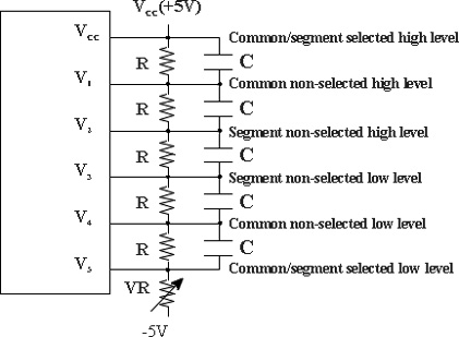
The necessary bias voltages are usually generated by the use of a resistor dividing network, and example of which is shown below. Vcc is usually 5 volts, and the number of resistors in the ladder is determined from the table above.
The values of the resistors is determined mostly by power requirements and waveform distortion. Because an LCD is a capacitive load, the values should be decreased to decrease distortion. However, this increases power consumption. These values should therefore be made as large as possible, keeping in mind that very large displays have very large capacitance, and may require lowering the resistor values.
Retaining the desirable liquid crystal display characteristics of ultra low power consumption and high contrast ratio under high ambient light levels, multiplexed liquid crystal displays greatly reduce the number of external connections necessary for numeric and mixed numeric descriptor displays and make possible dot matrix displays for full alphanumeric and graphic capability. Unlike conventional LCDs which have separate external connections for each segment and descriptor location plus common plane, multiplexed LCD's have their segments arranged as intersections of an X-Y grid. This reduction in the number of external connections enhances device reliability and potential display density. Their liability is the increased complexity of drive circuitry (or perhaps microprocessor software) necessary for their operation.
Unlike other display technologies that respond to peak or average voltage and current, Liquid Crystal Displays are sensitive to the RMS voltage across the interplane capacitance at a given segment location. In general, for a given liquid crystal fluid operating in a multiplex mode, as the number of "common planes" (i.e. electrodes common to all character locations - the "X" dimension of the matrix) is increased, the angle of view over which good display contrast is visible, decreases. When the multiplex rate is greater than about 16, it is necessary to switch to an STN display to maintain viewing angle and contrast. This applications note is applicable to both TN and STN displays, although for simplicity, we will show examples of a segmented display, and a 5x7 dot matrix only.
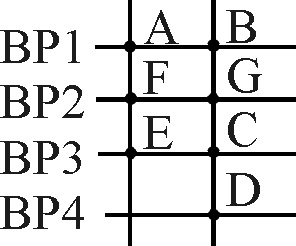
Three matrix formats have emerged as popular configurations. The 2 x 4 format, shown in FIGURE 1 below, is useful in numeric displays utilizing seven segments plus decimal point at each character location. FIGURE 1(a) shows the interconnections on the common planes. Note that the same segments at each digit are bussed together. FIGURE 1(b) shows the interconnections of the segment planes, rendering the 2 x 4 matrix arrangement for each character location as illustrated in FIGURE 1(c). FIGURE 1(d) shows the method by which four descriptors may be handled as a 1 x 4 subgroup in the same display.
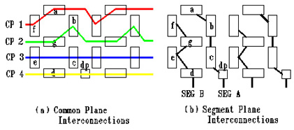
FIGURE 1
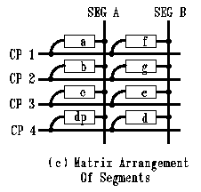
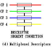
FIGURE 2 below illustrates the 5x7 dot matrix format. Seven common plane rows plus five segment plane columns per character form a 35 dot field which can be used for full alphanumeric capability. With this format, the matrix is physically arranged as a rectangular grid.
FIGURE 2
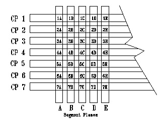
Other multiplex formats are possible for application to custom display requirements, consistent with limiting one dimension of the matrix to a practical value, and consistent with that which is possible in the geometric sense, i.e. there must be room to get all of the leads to the edge of the glass without crossing each other. Our technical question What is Direct Drive Multiplexing? shows a simple routing scheme.
The method of drive for multiplexed displays is essentially a time division multiplex with the number of time divisions equal to twice the number of common planes used in a given format. As is the case with conventional LCDs, in order to prevent irreversible electrochemical action from destroying the display, the voltage at all segment locations must be caused to reverse polarity periodically so that zero net DC voltage is applied. This is the reason for the doubling in time divisions: Each common plane must be alternately driven with a voltage pulse of opposite polarity.
|
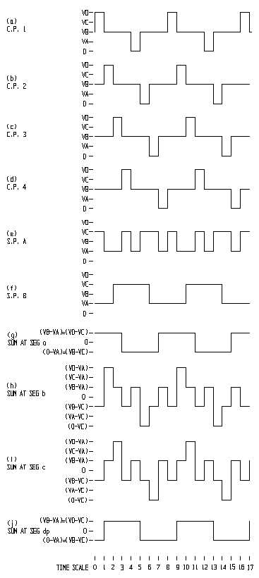
Refer to the figure at the right, which is representative of the 2 x 4 format, where the waveforms required for the generation of character "4" are given. In (a), (b), (c), and (d), the invariant common plane drive waveforms are shown. They can be thought of as bipolar strobe or select pulses. The segment plane waveforms corresponding to the specific characters "4" are presented in (e) and (f). The algebraically summed voltage at segment locations a, b, c, and d.p. for on and off optimized voltages are shown at (g), (h), (i), and (j), respectively (Refer to FIGURE 1). Voltage level VB is the datum reference for the display. To meet the symmetry criterion, no net DC voltage on the display, note that: (1 ) (VD - VB) = - (0-VB) (1a) VB = VD/2 (2) (VC - VB) = - (VA - VB). This convention of voltage levels is chosen consistent with the requirement that the display be driven from a logic system. (CMOS, capable of switching analog voltage levels) operating from a unipolar supply of magnitude >= VD. |
To determine the optimum ratio of (VD - VB) to (VC - VB), or identically (0 - VB) to (V A - VB), requires analysis of the mathematical expressions for the net RMS voltages impressed upon segment locations for both the on and off conditions.
In general, for a multiplexing scheme of N common planes and the conventions specified above:
|
(3) VRMS (OFF SEGMENT) = [(3+N)/4N * VD2 - (1 + N)/N VCVD + VC2] 1/2 |
|
(4) VRMS (ON SEGMENT) = [(N - 1)/4N * VD2 + (1 - N)/N * VCVD+VC2] 1/2 |
Optimum display contrast will occur when the ratio of the above expressions is maximized. This is determined by setting the derivative of the RMS ratio equal to zero and solving for VC in terms of VD. Our technical question What is Contrast shows how contrast is measured. Applying the formulae:
|
(5) d/dx u/v = (v du/dx -u dv/dx) /v2 |
|
and (6) d/dx un = nun -1 du/dx renders |
|
(7) VC = VD/2 (1 + 1/N1/2 ) |
|
for maximum RMS voltage ratio and hence, contrast. |
Substituting equation (7) into equations (3) and (4) provides expressions for optimized RMS on and off voltages:
|
(8) VRMS OFF(optimized) = VD ((1 - 1/ N 1/2) /2N ))1/2 |
|
(8a) VD = .VRMS OFF ((2N/(1 - 1/N1/2))1/2 |
|
and (9) VRMS 0N(optimized) = VD((1+1/ N1/2)/2N))1/2 |
|
FIGURE 4 |
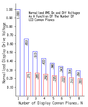
FIGURE 4 at left is a histogram plot showing normalized values of VRMSon and VRMS off (i.e. VD = 1.000) showing the interdependence of available drive voltage and the number of common planes. Note that as the number of common planes is increased, the contrast versus voltage requirement for the liquid crystal fluid used in such a format becomes more stringent. To actually use a given liquid crystal fluid in a given multiplex format requires matching of the fluid's turn on threshold voltage to the drive system's RMS off voltage. Utilizing equation (8a) by substituting the liquid crystal fluid's threshold voltage for V RMS Off will specify a minimum value of VD and thus a minimum supply voltage for the driving logic. |
Figure 5 below shows a typical voltage divider network suitable for providing the analog voltage levels to a multiplexed display via CMOS analog switching. Resistors RA, RB, RC and RD set the voltage ratios. Potentiometer RE sets the magnitude of VD to match the liquid crystal requirements. Capacitor Cbypassensures that node VD is of low source impedance at the drive frequency (i.e. at fdrive XC << RD), providing symmetric source impedances at the taps of the divider. Under these conditions, the highest impedance tap is at VB and is approximately equal to:
(10) (RA+RB)/2 = (RC + RD)/2 = ZsourceVB
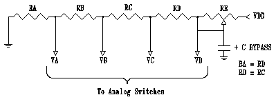
FIGURE 5
As is the case with non multiplexed displays, the drive frequency should be chosen to be above the flicker-fusion rate, i.e. >30 Hz. Since increasing the drive frequency significantly above this value increases current demand by the CMOS drive electronics, and to prevent problems due to the finite conductivity of the display segment and common electrodes, an upper drive frequency limit of 60-90 Hz is recommended. With these frequency limits in mind, the approximate source impedance of the divider network can be determined as a function of the net capacitance of the display to be driven. Because this capacitance is a function of the dielectric anisotropy of the liquid crystal fluid, it is non-linear with voltage and should be taken at its maximum value for the fully "on" condition.
Since the exact loading at each divider network voltage tap is a complex function of the instantaneous common plane drive, segments energized, and segments unenergized, the following rule of thumb is suggested as a method of choosing appropriate network source impedances. The RC time constant formed by the source impedance of node VB and the total "on" capacitance of the display should be an insignificant fraction (e.g. <1/100) of the common plane pulse width.
Recalling equation (10), the rule of thumb becomes:
|
(11) ((RC + RD)/2) CON <= 1/50 t |
|
where t is the common plane pulse width and is equivalent to: |
|
(12) 1/2N f Drive |
|
since (13) (VC - VB) = (RC/(RC + RD))(VD - VB) |
|
substituting equations (1a) and (7) yields: |
|
(14) RD = RC (N1/2 - 1), |
|
and combining (11), (12), and (14) results in: |
|
(15) RC < 1/(50 N3/2 fDrive Con ) |
For example: let
N = 3 (e.g. 3 x 3 format), fDrive = 40Hz (suggested nominal), Con = 3.8 nf, VTH = 2.3 VRMS ( LC fluid threshold)
|
Thus, by equation (15) RC = RB = 25.3K ohm |
|
Utilizing equation (14) RD = RA = 18.5 K ohm |
|
(16) |Xc BYPASS| = RD/100 @ fDrive or CBYPASS = 21..5 uf |
|
Utilizing equation (8a) VD = VRMS off ((2N/(1 - 1/N1/2))1/2 = (2.3V) (3.77) = 8.67 V |
As is the specification for non-multiplexed displays, the net DC component to which a segment location can safely be subjected is <50mV. A worst case analysis of resistor tolerances shows that if RA, RB, RC and RD are 1% film units, the criterion is met.
If a multiplexed LCD is to be operated over a temperature range in excess of the normal indoor ambient range of 18oC to 25oC, temperature compensation such that VRMSoff tracks the fluid threshold voltage Vth, may be required. Depending upon the particular liquid crystal fluid, the temperature coefficient of Vth is typically in the range of -5 to -15 mV/oC. Re-inspection of equation (8a) shows the relation between the temperature coefficient of VRMS "OFF" and that of VD: The right hand term of equation (8a) must be multiplied by the temperature coefficient of Vth to determine the temperature coefficient of VD. Note that this resultant is dependent upon the particular multiplex format utilized.
Thus, in summary, considerations of:
|
1. symmetric drive
|
are the constituents of the successful application of multiplexed LCDs.
Advanced Multiplex Derivation
|
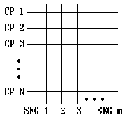
Let us assume a matrix arrangement of segments N x m. In the drawing on the right, the horizontal lines labeled CP1, CP2, etc. represent the common planes of a display multiplexed by N, and the vertical lines labeled SEG1, SEG2, etc., represent the N segments in the display. |
|
|
|
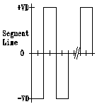
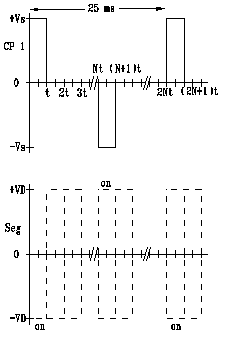
Let us further assume a time division scheme whereby time sequential "select" or "strobe" pulses are applied to the common planes (N dimension of matrix) at some arbitrary amplitude Vs. Refer to drawing on left. On the segment lead, we place an arbitrary voltage +/- VD, so that when it is summed with strobe pulse Vs sum (VS + VD) causes a segment location to turn on, and sum (VS-VD) causes a segment location to turn off. Refer to drawing on right. Symmetric levels +/- VD are chosen as a consequence of the (N -1) time intervals when the strobe pulse is not present. If asymmetrical levels are chosen, a higher residual voltage will be present on unaddressed segments. |
|
Twisted nematic liquid crystals are RMS sensitive. RMS voltage is proportional to the power that a voltage waveform can impart to its load:

The net RMS voltage seen by segment locations within the display can be calculated:
|
For an "on" segment: VRMS = [((VS + VD)2 + (N - 1)(VD)2)/N]1/2 |
|
For an "off" segment: VRMS = [((VS - VD)2 + (N - 1)(VD)2)/N]1/2 |
The optimum drive situation occurs when the above expressions achieve their maximum ratio. A little differential calculation is used to determine this maximum, which will yield:
|
VRMS = ((VS)2/N)1/2 * VS/N1/2 |
REMOVAL OF D.C.
|
|
The above scheme will impart DC voltage to the LCD. To correct this, all voltage polarities are inverted on alternate scans. In the timing diagram on the top left, the common plane voltage is shown to reverse polarity every N timing divisions. The resulting net DC voltage over a complete cycle is therefore 0V. In the segment waveform shown at the bottom left, the voltage applied to a given segment is somewhat more complicated because multiple segment drive signals are present. Our segment will only be turned on when the two waveforms are combined, and the resultant total RMS voltage exceeds the threshold voltage of the fluid used. |
|
|
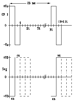
An alternate and functionally identical scheme is also used wherein the alternate polarity pulse pairs are applied in each scan through the commons. These waveforms are essentially the same as in the above example except that the positive and negative pulses occur during consecutive clock cycles. The resultant DC voltage is still 0V. The display segment still turns on during periods where the total RMS voltage is greater than the threshold voltage of the fluid, which now happens on successive clock cycles. |
LEVEL SHIFTING
|
|
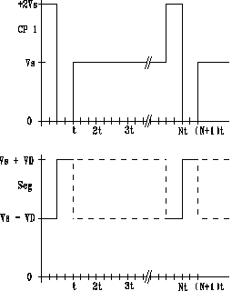
Because of these constraints, level shifting is applied to the bipolar waveforms discussed above. In the most basic form, a constant voltage of magnitude VS is added to all voltage levels, shifting them to the range 0 to + 2VS, which is compatible with the drivers: |
|
|
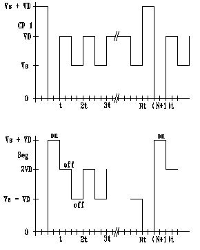
In a more advanced form, level shifting in an amount equal to VD is applied during the intervals when the strobe pulses are positive and in an amount equal to VS when the strobe pulses are negative. This system requires one additional voltage level but provides a real economy of overall supply voltage, reducing it from 2V S to VS + VD. This can be a 20% to 35% reduction depending on N. |
In all the above systems the voltage levels required are obtained from a resistive voltage divider. These resistors may be chip external making the system reconfigurable for different N's, if the driver is also reconfigurable. The resistors may also be internal to the chip . The taps off the resistive divider are controlled and switched to the display electrodes by a structure known interchangeably as an analog switch, a bilateral switch or a transmission gate. These act as an interfaces between the normal logic level control signals and the analog levels applied to the display. See our Multiplexing Liquid Crystal Displays app note for a discussion of these divider networks.
The supply voltage required for a given system depends on the LC threshold voltage, N, and the level shifting system used. The expression for the RMS off voltage must be made to match the threshold voltage of the LC fluid. Since the LC threshold voltage has a specific temperature coefficient, the overall supply voltage must be adjusted to track this temperature compensation for wide temperature excursions. The RMS "OFF" voltage in a given system is some constant fraction of the overall supply voltage. Since this fraction must track the LC threshold voltage, the temperature compensation of the threshold voltage must be multiplied by the inverse of the fraction to determine the ultimate temperature compensation of the supply voltage.
Temperature sensing is most easily accomplished with a sensor with a linear characteristic . A small buffer amplifier is generally required to interface the sensor to the output provisions in the display driver. Depending on those provisions, the buffer amp may need to feed the + or - chip power supply or the + or - end of the resistive divider.
THERMAL COMPENSATION
Due to the contrast versus voltage versus temperature characteristics of liquid crystal fluids and the sensitive nature of display drive voltage during multiplex operation, it becomes necessary to compensate LCD drive voltage for applications where the display is subjected to wide temperature excursions. For a typical twisted nematic liquid crystal fluid with a negative temperature coefficient, an under voltage condition with diminished display contrast will result at low temperatures and a "ghosting" or over drive condition will occur at high temperatures if no compensation techniques are employed. That which follows is a discussion of a practical method of providing first order linear compensation, compatible with most available driver circuits. Two examples are presented:
The first factor that needs to be determined in a particular application is the relationship between display RMS "OFF" voltage and display driver circuit supply voltage. Since different drive schemes are utilized, e.g. 3, 4, and 5 voltage level drive arrangements, this is best determined from the manufacturer's data sheet. Also required are the temperature coefficient and threshold voltage of the liquid crystal fluid. The fluid temperature coefficient must be divided by the ratio of RMS "OFF" voltage to driver circuit supply voltage to calculate the ultimate temperature coefficient of the driver circuit supply voltage. In this way the display RMS "OFF" voltage will track its optimum value over the temperature range.
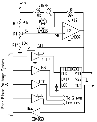
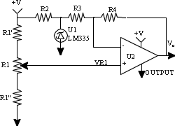
Figure 6 below shows the basic temperature regulation circuit. The heart of the circuit is U1, a National Semiconductor LM335 monolithic temperature sensor, which should be placed in physical contact with the LCD. The LM335 has a basic output voltage coefficient of 110mV/oC. Resistor R2 supplies operating current to U1, 1 mA nominal. Difference amplifier U2 inverts and scales this coefficient consistent with LCD/driver requirements. Potentiometer R1 provides a means by which the display operating voltage can be set. Note that range limiting resistor R1' and R1" may be added to increase the resolution of R1 and to determine suitable end points. Operational amplifier U2 may be any type capable of supplying sufficient output current to power the display driver circuit(s). An LM307 is a good choice for small systems since its output can swing close to the supply rail, minimizing the magnitude of the positive supply required. R1 must be fed from a regulated supply to maintain a stable output voltage at U2.
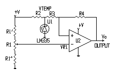
FIGURE 6
EXAMPLE #1
| Temperature Range: | -10oC to +60oC |
| Multiplex Mode: | 5x7 |
| Liquid Crystal Fluid: | Threshold Voltage: 2.30 Vrms @ 20oC |
| Temperature Coefficient of Threshold: | -8.0 mV/oC |
This drive uses the basic "1/2 select" scheme (4 voltage levels and reference as described earlier). As such, the display RMS "OFF" voltage is .211 times the overall driver supply voltage, for n = 7. The temperature coefficient of the supply voltage can be calculated:
|
-8.0 mV/oC/.211 = 37.9 mV/oC |
The driver supply voltage at the temperature limits can be computed from the display threshold voltages at those limits:
|
@ -10oC VTHRESH = 2.30 + (-8.0mV/oC *-30oC) = 2.54 Vrms |
|
@ +60oC VTHRESH = 2.30 + ( - 8.0 mV/oC * + 40oC) = 1.98 Vrms |
|
@ -10oC VSUPPLY = 2.54/.211 = 12.0 volts |
|
@ +60oC VSUPPLY = 1.98/.211 = 9.38 volts |
Referring to FIGURE 7 below, let R3= 10K, then R4 = 39K to determine the proper temperature coefficient at the output of U2. From the specifications of the LM335 device, it is found that its output voltage is 2.98 +/- .06 volts at 25oC. Using the basic op amp closed loop gain equation:
|
V0 = (R4/R3 + 1) VR1 - (R4/R3) VTEMP, |
|
Resolved for R1: VR1 = Vo + (R4/R3)VTEMP/( R4+ 1)/ R3 |
|
VR1 should be in the range of 3.95 to 4.05 volts considering the tolerance of U1. Choosing R1 =5K, R1' = 39K, and R1" = 18K allows VR1 to be varied +/- .5 volts, which is more than sufficient range. Since U2 must swing to +9.2 volts output at the low temperature limit, its positive supply is chosen at +12 volts. R2 can now be determined to be ~10K to allow 1 mA nominal current flow into U1. Also shown in FIGURE 8 is a method of level translation from standard 5 volt logic to the temperature controlled voltage of the drivers. U3, an RCA CD40109, low to high voltage converter, translates the incoming control signals. U4A, one-sixth of a CD4060 buffer, allows a high to low voltage logic conversion for the interrupt line feeding back to the main system. |
FIGURE 7
|
Level conversion by returning VSS to a negative voltage is suggested in the HLCD 0638/0539 data sheet. If the input is assumed to be standard 5 volt logic (HLCD 0538/0539 VDD terminals tied to +5 volts), VSS may go as negative as -1.67 volts before input logic level constraints are violated. This net driver circuit supply voltage of 6.67 volts maximum corresponds to a display temperature of 56.7oC minimum-clearly an unacceptable constraint.
EXAMPLE #2
| Temperature Range: | -10oC to +60oC |
| Multiplex Mode: | 3 x 3(6 x 3 for ICM 7233,7234) |
| Liquid crystal fluid: | Threshold Voltage: 2.30 Vrms @ 20oC |
| Temperature Coefficient of Threshold: | -8.0 mV/oC |
This family of drivers uses the "1/3, select" format of multiplex drive (3 voltage levels and reference). The display RMS "OFF" voltage is .333 times the overall driver internal resistor string voltage. Note that the negative end of the resistor string is brought out separately from the device's V SS terminal. The temperature coefficient of the display supply voltage can be calculated:
|
-8.0 mV/oC / .333 = 24mV/oC |
The display supply voltage at the temperature limits can be computed from the display threshold voltages at those limits:
|
@ + 10oC VTHRESH = 2.30 + ( - 8.O mV/oC * -10oC) = 2.38 Vrrns |
|
@ + 55oC VTHRESH = 2.30 * ( 8.0 mV/oC * +35oC) = 2.02 Vrms |
|
Thus: @ + 10oC VDisply supply = 2.38/.333 = 7.15 volts |
|
@ +55oC VDisplay supply = 2.02/.333 = 6.10 volts |
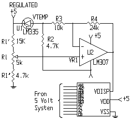
|
Figure 8 |
FIGURE 8 at left shows a modified form of the basic temperature compensation circuit in which U1 and R2 are reversed in position. This inverts the sense of voltage VTEMP so that the output of U2 goes more positive with increasing temperature to accommodate feeding the negative end of the display drive divider string. Resistor R3 is once again assumed at 10K, this time rendering R4 at 24K to match the required display voltage temperature coefficient. Recalling the resolved op amp closed loop gain equation from the previous example, VR1 is found to be in the range of 1.39 to 1.47 volts, taking into account the LM335 output voltage tolerance. Choosing R1 = 5K, R1' = 15K and R1" = 47K provides more than adequate adjustment range. |
Note that at the low temperature design limit the overall display divider supply voltage goes to 5.34 volts The driver data sheet states that the voltage at terminal VDISP must not go any more negative than 0.3 volts below system ground (VSS). If this driver is operated from a standard 5 volt logic system, this indicates a small discrepancy (.04 volts) in the display divider supply voltage, raising the minimum acceptable low temperature limit to + 11.7oC at specification. If lower temperature operation is contemplated using this family of drivers, the more elaborate level shifting scheme utilizing the CD40109 is required to keep the drivers within their specifications.
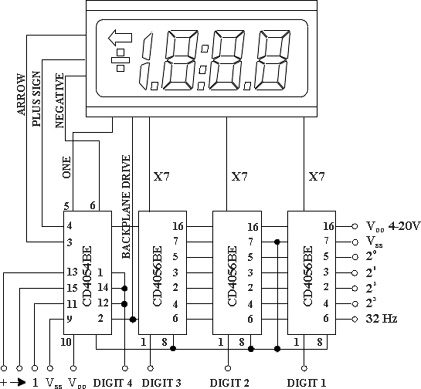
The example circuit below shows a typical application of direct drive decoder/driver ICs for numeric displays.
Required signals are 4 bits of BCD data, digit strobe, annunciator bits and square-wave display drive - the 32 HZ input shown on the drawing. The circuit is expandable for displays with more digits or annunciators.
See the IC Link Page for information on obtaining this or many other IC's for direct driving LCD's. Our Applications Note Direct Driving an LCD has additional basic direct drive information.
The example circuit below shows a typical application of multiplex controller/driver ICs for alphanumeric displays. The Hitachi HD44780 easily interfaces with common 4 or 8 bit microprocessors and is fully programmable for font size, duty cycle and display functions such as blinking, clearing and shifting. The character generator is capable of fixed or programmable fonts, including Japanese kana characters. By itself the HD44780 can control a display with either one or two 8-character lines.
This example is typical of Hitachi and compatible devices. See the IC Link Page for information on obtaining these chips.
All LCD drive voltages are generated on-chip with the assistance of a simple resistor divider shown in detail on our page Multiplexing LCD's. These divider networks are somewhat complicated to design, a call to our engineering department at 1-800-786-8710 may be of help during your design efforts.
Due to the contrast versus voltage versus temperature characteristics of liquid crystal fluids, and the sensitive nature of display drive voltage during multiplex operation, it may become necessary to compensate the LCD drive voltage for applications where the display is subjected to wide temperature excursions. For a typical Twisted Nematic Liquid Crystal Fluid with a negative temperature coefficient, an under voltage condition with diminished display contrast will result at low temperatures, and a "ghosting" or overdrive condition will occur at high temperatures if no compensation techniques are employed.
The first factor that needs to be determined in a particular application is the relationship between display RMS "OFF" voltage, and display driver circuit supply voltage. Since different drive schemes (Mux rates) are utilized, this is best determined from the manufacturer's data sheet. Also required are the temperature coefficient and threshold voltage of the liquid crystal fluid. (Assistance in selecting the correct LCD fluid for your application is available from LXD's application engineering department at (440)786-8700).
To calculate the ultimate temperature coefficient of the driver circuit supply voltage, the fluid temperature coefficient must be divided by the ratio of RMS "OFF" voltage to driver circuit supply voltage. In this way, the display RMS "OFF" voltage will track its optimum value over the temperature range.
The figure below shows the basic temperature regulation circuit. The heart of the circuit is U1, a National Semiconductor LM335 monolithic temperature sensor, which should be placed in close proximity to the LCD. The LC335 has a basic output voltage coefficient of 110mV/C. Resistor R2 supplies operating current to U1, 1mA nominal. Difference amplifier U2 inverts and scales this coefficient consistent with LCD driver requirements. Potentiometer R1provides a means by which the display operating voltage can be set.

Note that range limiting resistor R1' and R1" may be added to increase the resolution of R1 and to determine suitable end points. Operational amplifier U2 may be any type capable of supplying sufficient output current to power the display driver circuit(s). An LM307 is a good choice for small systems since its output can swing close to the supply rail, thus minimizing the magnitude of the positive supply required. R1 must be fed from a regulated supply to maintain a stable output voltage at U2.
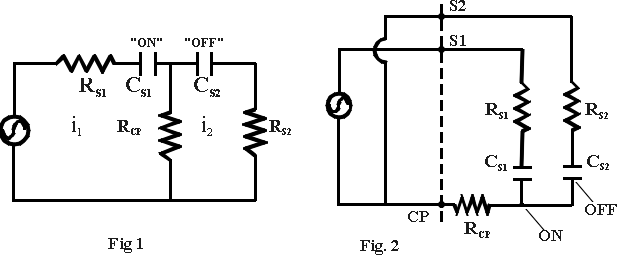
The most basic display configuration that will render ghosting is a two segment display in which one segment is energized and the other segment is driven with a signal identical to that which is applied to the display common plane, normally the "off" condition. As drive frequency and/or voltage are increased, the "off" segment starts to turn "on". FIGURE 1 below is a schematic of such a configuration.
Presented below are the electrical models used to characterize the mechanism of ghosting in such an LCD. In this model RS1 and R S2 are the segment resistance of segments one and two, and CS1 and CS2 are the capacitances of segments one and two. Resistance RCP represents the effective series resistance in the common plane circuit, consisting of contributions by the common plane electrode and lead-out, the crossover conductors, the common plane lead-out on the segment plane glass, and the substrate to terminal pin interface.
Segments are modeled as capacitors (with a non-linear liquid crystal dielectric), and with series resistances representing the resistivity of the segment electrodes. In the real display there are actually contributions by both electrodes, but for this argument it will suffice to lump them together for each segment.
FIGURE 2 below is simply FIGURE 1 redrawn to make the two-loop nature of the circuit more evident. Loop current i1 flows through the "on" segment impedances and common plane resistance RCP. Loop current i2 flows through the "off" segment impedances and RCP . From this it can be seen qualitatively that the magnitude of RCP determines the amount of voltage that reaches the "off" segment and causes ghosting. Note that because the display is always operated below the break frequency of network RS1 - CS1, ghosting will be a function of frequency as a result of the changing reactance of CS1 with frequency. If RCP were zero, ghosting could never occur. If RCP were infinite (i.e. common plane open), the "on" and "off" segments are in series, sharing the drive voltage according to the relative magnitude of their impedances. This happens when a crossover connection fails.
In a display consisting of a great number of segments, the electrical model must be expanded to account for contributions of RCP which may be different for each segment location. In general however, the worst case condition for ghosting will occur when all but one segment are turned "on" and the remaining segment is driven "off". This maximizes the voltage drop across RCP, which causes the "off" segment to see maximum voltage.
LXD specializes in the manufacture of extremely long life LCD's for those applications in which service life and reliable performance outweigh all other considerations. Our long life LCD's, with temperature ranges as low as -55oC and as high as 122oC, are designed for outdoor applications and others where extremes of temperature and humidity are encountered. These include gasoline pumps, marine instruments, oil exploration devices, and many others.
Our processes have been designed to eliminate two major types of display failures. These include "functional" failures that can be traced to defects in materials or process, and failures that are characteristic of a display's end of life behavior.
The incidence rate of both types of defects in normal manufacturing is not high, but since the cost of replacing a display can be twenty times its initial cost, and even higher in some outdoor applications, many users prefer an assured longer service life. The higher purchase price usually results in a lower cost of ownership.
"Functional" field failures, typified by seal failures, shorts, open segments, and ghosting, have been eliminated through manufacturing controls. Each type of defect was studied independently. Conditions or practices that permitted it to occur have been changed or eliminated. Early "end-of-life" failures (loss of alignment, bloating, high current) have also been eliminated through the use of state-of-the-art materials and the development of improved chemical processing and formulations.
LVDS is a differential signal system that is typically used for high speed data rate transfer. LVDS is not an interface protocol, but rather the hardware mechanism that is used to transmit the data across wires. This system can be used with either serial or parallel or a hybrid interface protocol.
The operation basically has the LCD controller transmitting two logic voltage levels that are compared in the LCD module. LVDS uses the difference in voltage between the two lines to encode information. These two lines are typically twisted pairs. The transmitter sends a small current into one line or the other, depending on the logic level to be sent. The current passes through a resistor which is matched to the impedance of the line at the LCD module, then returns in the opposite direction along the other wire. The LCD module senses the polarity of the voltage across the resistor to determine the logic level.
This type of signal minimizes the amount of radiated electromagnetic noise and power lost to conductor resistance. LVDS is less susceptible to noise than single wire data systems because it uses two wires with opposite current/voltage swings instead of the one wire used in single-ended methods to convey data information. The advantage of the differential approach is that if noise is coupled onto the two wires, the noise appears on both lines equally, and is mostly self-cancelling. The op amp at the receiver/LCD module end basically only looks at the difference between the two signals. Using this differential convention, the signals also tend to radiate less noise than single wire data signals due to the canceling of the induced magnetic fields. Constant current drivers are also not prone to ringing or switching spikes, which further reduces noise.
How LVDS Works
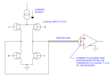
The schematic diagram shows a simple LVDS driver and receiver. It consists of a current source that drives the differential pair lines and an op amp receiver with high input impedance. This causes most of the driver current to flow through the termination resistor, which generates a voltage across the receiver inputs. When the driver switches, it changes the direction of current flow across the resistor, which changes the voltage sense from positive to negative, which creates a logical "one" or "zero".
LCD Module Protocol Interfaces
LCD controllers use familiar interfaces. Some controller ICs have more than one interface option that is user selectable. In many cases, the module LXD supplies to you will already be internally configured to your interface requirements. As an LCD module manufacturer, LXD welcomes discussions about various module design parameters, including different interface options.
All interface protocols must initialize the LCD module when it is first energized prior to use.
The most common LCD Module Interface Protocols are:
The parallel interface typically controls the LCD via 8 data pins and 3 control lines. The control lines used are Enable (E), Register Select (RS), and Read/Write (R/W). RS tells the LCD module if the information being sent is an Instruction or Data. The Enable tells the LCD module that the data or instruction in the register is ready to be interpreted by the LCD Module. Some controllers may have more than one Enable Control Line. The Read/Write tells the module whether to write data or read data from the register.
In addition to the common interface connections presented as examples here, some modules may include additional control lines. Some examples are:
V0 - Contrast Adjustment, which adjusts the voltage applied to the LCD
CS - Chip Select
BUSY - Typically a low state indicates busy state
Parallel Interface Types
Some parallel interface connection examples are:
8-Bit Parallel
| Designation | Description | Function |
|---|---|---|
|
RS |
Register Select |
Control line L: Instruction H: Data write |
|
R/W |
Read/Write |
Control line L: Data Write, H: Data Read |
|
E |
Enable |
Control line - Allows information to be interpreted |
|
D0 |
Data Line |
8 Bit Parallel Data Lines |
|
D1 |
Data Line |
|
|
D2 |
Data Line |
|
|
D3 |
Data Line |
|
|
D4 |
Data Line |
|
|
D5 |
Data Line |
|
|
D6 |
Data Line |
|
|
D7 |
Data Line |
4-Bit Parallel (Common for QVGA monochrome display modules)
| Designation | Description | Function |
|---|---|---|
|
FLM |
First Line Marker |
Control line - Frame Signal |
|
DISP OFF |
Display Off |
Control line L: Display Off, H: Display On |
|
M |
Control line - AC signal for Display Driver |
|
|
CL1, LP |
Latch Pulse |
Data Latch Clock Signal |
|
CL2, CP |
Shift Pulse |
Data Shift Clock Signal |
|
D0 |
Data Line |
4 Bit Parallel Data Lines |
|
D1 |
Data Line |
|
|
D2 |
Data Line |
|
|
D3 |
Data Line |
Serial Interface Types
o Serial - Serial Data In, Register Select, Reset, and Serial Clock
o SPI (Serial Peripheral Interface)
Timing and operation may differ from usual SPI
o I2C (Inter-Integrated Circuit) - Uses Serial Data Line and Serial Clock
Some interface connection examples are:
Serial
Serial LCD controllers typically have one Serial Data Line that writes data and cannot read. Normally, a Register Select Line (Sometimes designated A0) is used to tell the controller whether the incoming data is display information or a controller command
Serial interface example
| Designation | Description | Function |
|---|---|---|
|
SCL, SCLK, SCK, or CLK |
Serial Clock |
Control line (output from master) |
|
CS, CSn (n = chip selected, "1, 2, etc") |
Chip Select |
Control line L:Chip Selected, H:Unselected |
|
SDI, DI, SI, SDA |
Serial Data In |
Data Line |
|
A0 |
Register Select |
H: Data, L: Instruction |
|
RES |
Reset |
L: Enable, H: Disable |
When RES is enabled, the register settings are initialized or cleared.
SPI Interface
SPI, or Serial Peripheral Interface bus, is a synchronous (data is synchronized to the clock) serial data link standard that operates in full duplex mode, which means that devices that can communicate with one another simultaneously. To do this, two data lines are required. With this standard, devices communicate in a master/slave mode, where the master device (host processor) initiates the data and the clock. The LCD module is the (or one of the) peripheral slave device(s) attached to the data bus. Multiple peripherals (display modules and other devices) are addressed on the same serial data bus. However, the LCD module will only listen to the data it sees when the Chip Select line is active (usually low). If the Chip Select line is inactive (usually High), the LCD module listens to the data on the bus, but ignores it. The SDO line is not active when this state occurs.
The SPI bus is comprised of four logic signals, two control lines and two data lines and is commonly referred to as SPI (4 wire).
Serial SPI interface example
| Designation | Description | Function |
|---|---|---|
|
SCL, SCLK, SCK, or CLK |
Serial Clock |
Control line (output from master) |
|
CS, CSn (n = chip selected, "1, 2, etc") |
Chip Select |
Control line (not present for SPI 3-wire) |
|
SDI, DI, SI |
Serial Data In |
Data Line |
|
SDo, DO, SO |
Serial Data Out |
Data Line |
Occasionally, SDI (serial data in) may be called out as MOSI (Master Out Slave In) from Motorola's original name for these lines and MISO (Master In Slave Out) for SDO. The chip select line may be alternatively labeled SS (Slave-Select), or STE (Slave Transmit Enable). SPI is sometimes referred to as National Semiconductor's trademark Microwire, which is essentially a predecessor of SPI, which only supports half duplex.
With CS (Chip-Select) the corresponding peripheral device is selected by the LCD Controller. This pin is mostly active-low. In the unselected state the SDO lines are hi-impedance and therefore inactive. The clock line SCL is brought to the device whether it is selected or not. The clock serves as synchronization of the data communication.
The chip select signal CS is optional for a single device system, because you could tie the CS input at the LCD Module low, if the other lines are dedicated to SPI use. This is sometimes called a 3 Wire SPI Interface.
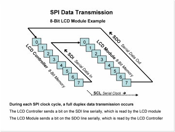
SPI Data transmissions usually involve two shift registers. Most display module applications normally use 8-bit words. However, different size words, such as 12 bit, are also used. By convention, the most significant bit is shifted out of one shift register while the least significant bit is shifted in. The word is then written into memory if the CS (chip-select) is low (active). If not, the data is ignored.
Since the SPI interface protocol is a de facto standard, many variations of the standard protocol are used. For instance, chip manufacturers may use some of the parallel data lines when configuring the IC driver chip for serial communication.
I²C (Inter-Integrated Circuit)
I²C uses only two bi-directional lines, Serial Data Line (SDA) and Serial Clock (SCL), which are both typically pulled up with resistors. Typical voltages used are +5 V or +3.3 V. One of the strengths of the I²C interface is that a micro can control multiple devices with just the two I/O pins and software.
Because of the I²C design, it is only half-duplex. The interface generally transmits 8-bit words, sending the most significant bit first.
RS232 Interface :
The RS232 serial interface uses 3 lines to control the LCD module. These are transmit, receive, and ground. This interface does not require the Enable and Register Select lines.
Some modules may include additional control lines. Some examples are:
C86 - Defines specific MPU interface. For instance, H: 6800, L: 8080
CS - Chip Select. For instance, H: Chip Unselected, L: Chip Selected
| Designation | Description | Function |
|---|---|---|
|
RST, RES |
Reset |
Control line L: Settings initialized |
|
E1 |
Enable 1 |
Control line - Allows Read/Write information to be interpreted |
|
E2 |
Enable 2 |
Control line - Allows Read/Write information to be interpreted |
|
R/W |
Read/Write |
Control line L: Data Write, H: Data Read |
|
A0/DI |
Register Select / Data In |
|
|
D0 |
Data Line |
8 Bit Parallel Data Lines |
|
D1 |
Data Line |
|
|
D2 |
Data Line |
|
|
D3 |
Data Line |
|
|
D4 |
Data Line |
|
|
D5 |
Data Line |
|
|
D6/SCL ** |
Parallel mode Data Line/ Serial Clock |
|
|
D7/SDI ** |
Parallel mode Data Line/ Serial Data In |
**Chip manufacturers will assign different functions to a specific bus connection, depending on whether the chip is configured for Parallel or Serial.
TFT Parallel Interface
| Designation | Description | Function |
|---|---|---|
|
DCLK, CK |
Data Sampling Clock |
Control line Data Sampling Clock Signal |
|
HSync |
Horiz Sync signal |
Control line - Horizontal Sync Signal (negative going) |
|
VSync |
Vertical Sync Signal |
Control line - Vertical Sync Signal (negative going) |
|
R0 |
Red Data Signal |
Data Lines |
|
R1 |
Red Data Signal |
|
|
R2 |
Red Data Signal |
|
|
R3 |
Red Data Signal |
|
|
R4 |
Red Data Signal |
|
|
R5 |
Red Data Signal |
|
|
GND |
Ground |
Ground lines are placed between various signal lines for isolation. Only 3 shown as examples |
|
G0 |
Green Data Signal |
Data Lines |
|
G1 |
Green Data Signal |
|
|
G2 |
Green Data Signal |
|
|
G3 |
Green Data Signal |
|
|
G4 |
Green Data Signal |
|
|
G5 |
Green Data Signal |
|
|
GND |
Ground |
|
|
B0 |
Blue Data Signal |
Data Lines |
|
B1 |
Blue Data Signal |
|
|
B2 |
Blue Data Signal |
|
|
B3 |
Blue Data Signal |
|
|
B4 |
Blue Data Signal |
|
|
B5 |
Blue Data Signal |
|
|
GND |
Ground |
|
|
ENAB |
Enable |
Control line - Horizontal Display Position Set Signal H: Enables LCD |
|
R/L Option may not be present |
Right or Left Scan |
Chip Specific - tied to VCC or GND |
|
U/D Option may not be present |
Up or Down Scan |
ChipSpecific - tied to VCC or GND |
|
V/Q Option may not be present |
VGA or QVGA |
Chip Specific - tied to VCC or GND |
Digital 18-Bit RGB-TFT Interface with Gamma Correction
| Designation | Description | Function |
|---|---|---|
|
DCLK |
Clock Signal Input |
Control line H: User can input different polarity CLK by EDGSL Setting L: User can select CLK Rising or Duel Edge to Latch by EDGSL |
|
EDGSL |
Define Input Clock Polarity |
Control Line L: Latch Data by Rising Edge of CLK (Default) H: CLK Polarity is Inverted, Latch Data by Falling Edge of CLK |
|
VCC |
Digital Power Supply |
3.3V Typical |
|
AVDD |
Analog Power Supply |
|
|
RESETB |
Hardware Global Reset |
L: Active, H: Default Pull High |
|
VGL |
Gate Off |
Control line - Gate Off Power Supply Voltage |
|
VGH |
Gate On |
Control line - Gate On Power Supply Voltage |
|
VCOM |
Common Voltage |
Common Electrode Voltage Input |
|
V1 |
Gamma Voltage level 1 |
|
|
V2 |
Gamma Voltage level 2 |
|
|
V3 |
Gamma Voltage level 3 |
|
|
V4 |
Gamma Voltage level 4 |
|
|
V5 |
Gamma Voltage level 5 |
|
|
V6 |
Gamma Voltage level 6 |
|
|
V7 |
Gamma Voltage level 7 |
|
|
V8 |
Gamma Voltage level 8 |
|
|
V9 |
Gamma Voltage level 9 |
|
|
V10 |
Gamma Voltage level 10 |
|
|
DE |
Input Data Enable Control |
When in DE mode, Active high to enable data input, Default Pull Low. |
|
R0 (LSB) |
Red Data Signal |
Data Lines |
|
R1 |
Red Data Signal |
|
|
R2 |
Red Data Signal |
|
|
R3 |
Red Data Signal |
|
|
R4 |
Red Data Signal |
|
|
R5 (MSB) |
Red Data Signal |
|
|
GND |
Ground |
Ground lines are placed between various signal lines for isolation. Only 3 shown as examples |
|
G0 (LSB) |
Green Data Signal |
Data Lines |
|
G1 |
Green Data Signal |
|
|
G2 |
Green Data Signal |
|
|
G3 |
Green Data Signal |
|
|
G4 |
Green Data Signal |
|
|
G5 (MSB) |
Green Data Signal |
|
|
GND |
Ground |
|
|
B0 (LSB) |
Blue Data Signal |
Data Lines |
|
B1 |
Blue Data Signal |
|
|
B2 |
Blue Data Signal |
|
|
B3 |
Blue Data Signal |
|
|
B4 |
Blue Data Signal |
|
|
B5 (MSB) |
Blue Data Signal |
|
|
GND |
Ground |
TTL-TFT Interface
| Designation | Description | Function |
|---|---|---|
|
DCLK, CK |
Data Sampling Clock |
Control line - Latch Data At Negative Edge Signal |
|
R0 (LSB) |
Red Data Signal |
Data Lines |
|
R1 |
Red Data Signal |
|
|
R2 |
Red Data Signal |
|
|
R3 |
Red Data Signal |
|
|
R4 |
Red Data Signal |
|
|
R5 (MSB) |
Red Data Signal |
|
|
GND |
Ground |
Ground lines are placed between various signal lines for isolation. Only 3 shown as examples |
|
G0 (LSB) |
Green Data Signal |
Data Lines |
|
G1 |
Green Data Signal |
|
|
G2 |
Green Data Signal |
|
|
G3 |
Green Data Signal |
|
|
G4 |
Green Data Signal |
|
|
G5 (MSB) |
Green Data Signal |
|
|
GND |
Ground |
|
|
B0 (LSB) |
Blue Data Signal |
Data Lines |
|
B1 |
Blue Data Signal |
|
|
B2 |
Blue Data Signal |
|
|
B3 |
Blue Data Signal |
|
|
B4 |
Blue Data Signal |
|
|
B5 (MSB) |
Blue Data Signal |
|
|
GND |
Ground |
|
|
DE |
Data Enable |
Control line - Horizontal Display Position Set Signal H: Enables LCD |
SPI-TFT Interface
| Designation | Description | Function |
|---|---|---|
|
SCL |
Serial Clock |
Control line SPI Serial Interface Clock |
|
HSync |
Horiz Sync signal |
Control line - Horizontal Sync Signal (negative going) |
|
VSync |
Vertical Sync Signal |
Control line - Vertical Sync Signal (negative going) |
|
RES |
Reset |
Reset Enable |
|
CS |
Chip Select |
SPI Chip Select |
|
SDO |
Serial Data Out |
SPI Serial Data Output |
|
SDI |
Serial Data In |
SPI Serial Data Input |
|
ENAB |
Enable |
Control line - Horizontal Display Position Set Signal H: Enables LCD |
|
DCLK, CK |
Data Sampling Clock |
Control line Data Sampling Clock Signal |
|
R0 |
Red Data Signal |
Data Lines |
|
R1 |
Red Data Signal |
|
|
R2 |
Red Data Signal |
|
|
R3 |
Red Data Signal |
|
|
R4 |
Red Data Signal |
|
|
R5 |
Red Data Signal |
|
|
GND |
Ground |
Ground lines are placed between various signal lines for isolation. Only 3 shown as examples |
|
G0 |
Green Data Signal |
Data Lines |
|
G1 |
Green Data Signal |
|
|
G2 |
Green Data Signal |
|
|
G3 |
Green Data Signal |
|
|
G4 |
Green Data Signal |
|
|
G5 |
Green Data Signal |
|
|
GND |
Ground |
|
|
B0 |
Blue Data Signal |
Data Lines |
|
B1 |
Blue Data Signal |
|
|
B2 |
Blue Data Signal |
|
|
B3 |
Blue Data Signal |
|
|
B4 |
Blue Data Signal |
|
|
B5 |
Blue Data Signal |
|
|
GND |
Ground |
LVDS (Low-Voltage Differential Signaling)
LVDS is a differential signal system that is typically used for high speed data rate transfer. LVDS is not an interface protocol, but rather the hardware mechanism that is used to transmit the data across wires. This system can be used with either serial or parallel or a hybrid interface protocol.
The operation basically has the LCD controller transmitting two logic voltage levels that are compared in the LCD module. LVDS uses the difference in voltage between the two lines to encode information. These two lines are typically twisted pairs. The transmitter sends a small current into one line or the other, depending on the logic level to be sent. The current passes through a resistor which is matched to the impedance of the line at the LCD module, then returns in the opposite direction along the other wire. The LCD module senses the polarity of the voltage across the resistor to determine the logic level.
This type of signal minimizes the amount of radiated electromagnetic noise and power lost to conductor resistance. LVDS is less susceptible to noise than single wire data systems because it uses two wires with opposite current/voltage swings instead of the one wire used in single-ended methods to convey data information. The advantage of the differential approach is that if noise is coupled onto the two wires, the noise appears on both lines equally, and is mostly self-cancelling. The op amp at the receiver/LCD module end basically only looks at the difference between the two signals. Using this differential convention, the signals also tend to radiate less noise than single wire data signals due to the canceling of the induced magnetic fields. Constant current drivers are also not prone to ringing or switching spikes, which further reduces noise.
How LVDS Works
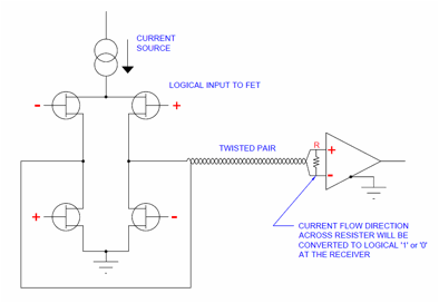
The schematic diagram shows a simple LVDS driver and receiver. It consists of a current source that drives the differential pair lines and an op amp receiver with high input impedance. This causes most of the driver current to flow through the termination resistor, which generates a voltage across the receiver inputs. When the driver switches, it changes the direction of current flow across the resistor, which changes the voltage sense from positive to negative, which creates a logical "one" or "zero".
TMDS (Transition Minimized Differential Signaling)
TMDS is a technology for transmitting high-speed serial data and is used by the DVI and HDVI video interfaces.
TMDS is similar to low-voltage differential signaling (LVDS) in that it uses differential signaling to reduce electromagnetic interference (EMI), which allows faster signal transfers with increased accuracy. Like LVDS, the data is transmitted serially over the data link.
Technical Q&A
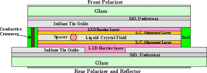
Cross-sectional view of a typical display.
Simply put, a liquid crystal display (LCD) is a parallel plate capacitor with a dielectric between the plates. However, it's not quite that simple. First we select glass coated with a transparent metal coating for the electrodes of the display. The glass is usually a soda lime type but in some instances it can be a more expensive borosilicate type. The transparent metal coating can be any thin layer of conductive material, such as gold, silver or tin. In order to keep the cost down and the have a reasonable process window with a highly transparent coating, the industry has been using indium-tin oxide (ITO) as the preferred electrode material.
Photoresist is then put on top of the transparent metal coating and a photolithographic process is used to image patterns in the photoresist. These patterns can be segments of numeric digits or they can be icons that represent various functions. The exposed patterns are then developed and the glass is sent through an acid bath where the excess metal coating is removed. The remaining photoresist is stripped off and the patterned segment and common plane electrodes have been generated.
After the electrodes have been made, an insulating layer is put on top of them. This is a silicon dioxide layer that is used to seal the electrode surface, act as an electrical barrier, and index match the electrodes and the glass. The next layer to be applied is the liquid crystal alignment layer. This is usually a polyimide type material and has been chosen for its environmental stability in high moisture and heat. More importantly is its ability to cause the molecules of liquid crystal to align their long axis in the direction in which the polymer has been buffed.
We then buff the two halves of the display at right angles to one another and since the liquid crystal molecules like to arrange themselves parallel to one another, we cause a helical structure to be formed between the two electrode faces. This helical structure is a 90 degree rotation of the liquid crystal molecules from one side of the display to the other. After the polymer is buffed, a glue ring or seal is printed on the glass. This is a thermoset epoxy type material with a very high glass transition temperature.
We then apply a small spot of conductive epoxy to connect the common plane electrode on the top piece of glass to the segment plane which is on the bottom piece of glass. This conductive epoxy is called a crossover dot.
To make the display uniform in appearance, spacers are then applied. These are usually glass rods that have the desired diameter to produce a fixed gap between the glass plates. Depending on the liquid crystal used, this gap can be between 6 and 8 microns. The two halves of the display are then heat sealed together. A very thin, uniform, flat and empty bottle has been formed.
A liquid crystal is put inside this bottle by using a vacuum filling technique. The liquid crystal (dielectric material of our capacitor) is selected for it's various physical properties. The application may call for a liquid crystal fluid that has a very low operating voltage or the display may be used outdoors and require a very wide temperature range. Display manufacturers have developed several liquid crystal mixtures to fulfill most applications.
Once the liquid crystal has been put inside the display and the port opening has been sealed, a polarizer is put on the front and an analyzer (another polarizer) is put on the back. If everything has gone as planned, we will have a device that can present the desired information to an observer. In other words, you will have a device similar to what is seen in calculators and gas pumps. With a little imagination, many variations of displays can be made.
See the above cross-sectional view of a typical display.
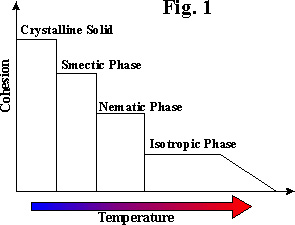
Liquid crystals are long chain organic molecules that exhibit the properties of a liquid yet have the long range ordering of a solid. The liquid crystalline state constitutes an intermediate phase or mesophase between solids and liquids. There are several types of liquid crystals and the ones used for displays are called thermotropic liquid crystals. As the name implies, thermotropic liquid crystals are affected by heat. If heat is added to the crystalline phase of the liquid crystal it will transition into the smectic phase (melting point), as more heat is added the liquid crystal will go through the nematic phase (used for display applications) and finally into the isotropic phase (clearing point) see fig 1.
Twisted nematic (TN), supertwisted nematic (STN) and active matrix (AMLCD) displays use the nematic phase for their operation. This phase is selected for its physical properties and the widest temperature range. It should be noted that the fluids used for display purposes are mixtures of several different liquid crystals. By mixing several liquid crystals together, a eutectic mixture will result with the melting point depressed well below room temperature.
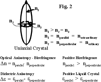
Liquid crystals are uniaxial. For example, if one measures the physical parameters of a water molecule, it can be shown that the data for that parameter would be the same no matter what direction the measurements were taken. Liquid crystals differ in that the value of the physical parameter is dependent on the direction it was measured relative to the molecule. We can measure the index of refraction of the molecule perpendicular to the long axis, and then parallel to the long axis, and the two values would be different, see fig 2. This is the index of refraction anisotropy of the liquid crystal or the birefringence. This would also hold true for the magnetic susceptibility, electrical conductivity, thermal conductivity, dielectric permitivity, and elastic constant.
Because liquid crystal molecules want to lie parallel to one another (orientational order) and they are uniaxial (anisotropic), we can exploit these properties to make useful devices.
As a practical matter, a given liquid crystal fluid is chosen using only a few critical parameters. The two most important are:
1) Working temperature range. - Most LCD fluids have a working temperature range of about -40c to +85c in a direct drive mode. As +85c is about +185 Fahrenheit, this temperature range covers the majority of both commercial and industrial applications. In applications where the display will be outdoor or in direct sunlight, a higher temperature range is recommended. Our #16 and #18 fluids are speciall formulated for extremely high temperature applications, and can withstand temperatures over +120c. On the low end, our #1 fluid can operate at temperatures as low as -55c.
2) Voltage Threshold - The supply voltage of your circuit determines the amount of drive voltage available to the display. In general, all of our fluids will work fine in 5V circuits in a direct drive mode. The problem comes in when you do not have 5V available, or the circuit is multiplexed.
For 3V applications, we have developed our #4 or our newer #19 fluids. These fluids have a somewhat lower threshold and will work fine at 3V either direct drive, 2:1, or 3:1 mux.
For highly multiplexed designs, the fluid selection becomes critical. The subject is somewhat complicated, but in general the higher the multiplex rate, the higher the voltage will need to be to drive a given fluid into saturation. The reason is that when you multiplex a display, each individual segment is time-division multiplexed, that is, you are only driving a segment for a portion of the total cycle. In a 3:1 mux, each pixel is only driven for one third of the time. The pixels are never really turned on all the way, and then they are left to turn off while other pixels are being driven. This results in greatly reduced contrast and viewing angle. Call our Engineering Department at 1-800-786-8710 for additional information.
Ordinary light from an incandescent bulb or from the sun is randomly polarized, that is, it includes waves that are oriented in all possible directions.
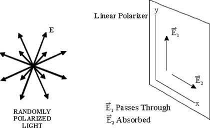
A polarizer is a material that is used to convert a randomly polarized ("un-polarized") beam of light into a polarized one, oriented in such a way that light with E2 (electric vector) along the x axis is absorbed, while the E1 along the y axis is transmitted. What emerges is that component of the original wave which had the y direction polarization. In the example above, the polarizing direction is along the y axis.
Positive image reflective liquid crystal displays have a polarizer applied to the front of the display and a reflector applied to the rear of the display. The liquid crystal molecules control the polarization state of beam of light polarized by the front polarizer. Controlling the orientation of the liquid crystal molecules will change the polarization of the beam.
As the polarized light from the front polarizer passes through an un-energized display, it will be rotated 90 degrees by the liquid crystal and either absorbed or passed by the rear polarizer. When the display segment is energized, the liquid crystal will rotate in the direction of the electric field and no longer rotate the polarized beam of light. Again, depending on the direction of the analyzer, the light will be either absorbed or passed. In the case of a positive image reflective display, this would produce a dark character on a light background. It is important to note that twisted nematic liquid crystal displays must have a polarizer applied to both the front and rear surfaces for them to function as useful devices.
The temperature range of any LCD is almost totally dependent on the fluid inside the display. For example, a display built using LXD's #6 LCD fluid, will have an operating temperature range of -40c to +105c when used in a direct drive mode. The storage temperature goes down to -55c. The temperature specifications for all our fluids are available in our section First Steps in Designing a Custom Display. In most applications, a temperature range of -40c to +85c is sufficient, however for unusual applications, LXD has fluids available with operational temperature ranges as low as -55C and as high as +122c .
The voltage threshold of a fluid is not linear across its entire temperature range. The result of this non-linearity is that you need to increase the drive voltage slightly at low temperatures for an acceptable response, and you need to lower the voltage at high temperatures to prevent "ghosting". A properly designed temperature compensation circuit should take care of both of these conditions so as to realize the stated temperature range. Voltage Vs Temperature curves are available for all LXD fluids.
The graph below shows the graph for LXD's #15 LCD fluid.
Call an LXD Applications Engineer (800)786-8710 for assistance (trying to explain it all here would be prohibitive.) An example of a basic temp compensation circuit is shown in our App Notes Section.
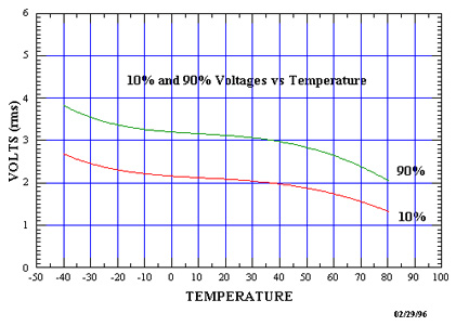
The rear polarizer of a reflective display includes a diffuse reflector, such as brushed aluminum. This layer reflects polarized ambient light that has entered the front of the display back trough the LCD cell. Reflective displays require ambient light to be seen. They exhibit high brightness, excellent contrast, and wide viewing angles. They are particularly suitable for use in battery operated equipment where an adequate level of light is always available. Reflective LCD's cannot be backlit, however they can be front lighted in some applications.
Transmissive displays have a clear polarizer on the front and the back. The display therefore depends on light coming through from the back of the display toward the observer in order to be seen. Most but not all transmissive displays are negative image, and we sometimes add colored filters to different areas of the display to highlight different annunciators.
Transflective displays have a rear polarizer which includes a translucent material which reflects part of the ambient light, and also transmits backlighting. As the name implies, it is a compromise between the transmissive and reflective viewing mode. Used in reflection, it is not as bright and has lower contrast than the reflective type LCD, but it can be backlit for use in low light conditions.
Pins, Heat Seals, and Elastomers are methods of mechanically interfacing the display to a printed circuit board.
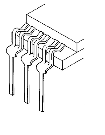
|
Pins are attached to the display to allow the user to either mount the display in a socket or solder it directly into a circuit board. From an end user standpoint, pins are the easiest to use since there is no requirement for a compression bezel or expensive heat seal bonding equipment.
The pins are attached to the glass with a structural epoxy on the back. On the top, we apply an electrically conductive epoxy with an RTV overcoating. Pins are the most reliable connection method. |
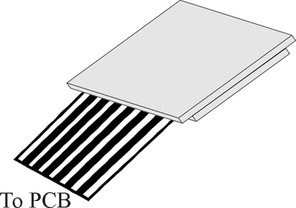
|
Heat seals are similar to flexible circuit boards with the difference being that the interface tabs are made of a conductive hot melt adhesive. Generally, particles such as carbon, gold, or silver are added to the adhesive to make it conductive. The pads of the heat seal are aligned with the pads of the display and a hot bar is brought down under pressure and the conductive adhesive is melted and bonded to the display. The adhesive is allowed to cool and an electrical bond is made with the display. |
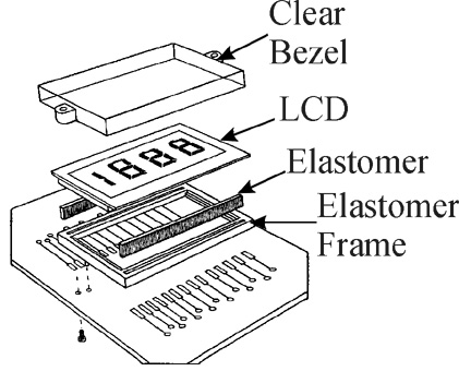
|
Elastomers are silicon strips of alternating conductors and insulators. These materials are generally soft and compliant and can be easily compressed between the display and circuit board. Elastomers require a bezel to squeeze the display and circuit board together. |
First I will explain what "First Minima" is, and then I'll tell you why it's important.
What is "First Minima"?
A "First Minima" liquid crystal display is one that is optimized for the thinnest possible cell gap for a specific liquid crystal mixture and a specific wavelength of light. Gooch and Tarry (1) showed that the transmitted light intensity can be described by:


where d is the film thickness (cell gap), Dn is anisotropy of refractive index of the liquid crystal, and l is the wavelength of light. For a standard twisted nematic display, q = p/2 or 90 degrees and Dn will be fixed by the liquid crystal mixture.
We can determine the proper cell gap for a given liquid crystal if we know the wavelength of light that is being used. For most applications, a wavelength of 550 nm (Green) is used since this is the center of the visible spectrum, and it is also the photopic peak of the human eye. See the figure below for a plot of transmission versus cell gap for a 90 degree twist, a Dn of .18, and wavelengths of 400 nm (blue), 550 nm (green), and 700 nm (red). From this plot we can see that there are minima for 550 nm (green) light at 2.65 micron, 5.92 micron and 9.0 micron. The first minima for this liquid crystal is 2.65 micron.
The graph below shows that a display can be optimized for only one wavelength at a time. This is important to know if one is contemplating a normally black (transmissive) display with several different colored filters or a backlight behind the display. During the design process, it is necessary to fully specify all colors. We can then optimize the cell gap for the most important wavelength (color).
1 J Phys D: Appl. Phys., Vol. 8, 1975, 1575-84
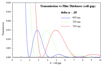
Why is this important?
Simply put, a "First Minima" display will have the maximum contrast and viewing angle possible for a given LCD fluid. So if you want the best looking display you can get, specify that it be built at the "First Minima". This phenomenon is not very important for a positive image display, but for a negative image display the difference is dramatic.
A logical question might be, "Why don't you just build every display at the "First Minima" so every display looks as good as it possibly can?" Good question, and the answer has to do with a manufacturing problems that come about because of the small cell spacing required for these cells.
The glass that we use to build displays is extremely flat, but it does have slight imperfections in it. These imperfections tend to be small bumps on the glass about 2-3 microns high. As can be seen on the graph above, the TOTAL cell gap in this display (the distance between the top and bottom sheets of glass) needs to be about 2.7 microns. It is therefore possible that a small bump on the top glass will touch a small bump on the bottom glass, resulting in a front to back short in the display. There is no way to prevent or correct these shorts, and these displays are simply discarded.
The answer to this problem is to develop a fluid that has a "First Minima" of about 5 microns or greater. At this wide cell gap front to back shorts are not a problem. We therefore have a win-win situation where you get a display with maximum contrast and viewing angle, and we can manufacture it without any yield fallout. As an added bonus, the first minima fluids cost about the same as the others, so there is no increase in price!
We have a few first minima fluids, our #6 and our #16. For all new TN designs, we usually specify the #16 fluid, as it also has a wider temperature range, and a more even color.
Twisted Nematic (TN) and Super Twisted Nematic (STN) are the terms used to describe two types of liquid crystal displays. TN displays have a twist ( the rotation of the molecules from one plane of the display to the other) of 90 degrees or less. All passive direct drive , active matrix, and most passive low level (x2 to x32) multiplexed LCD's have a 90 degree twist.
As the name implies, Super Twisted Nematic LCD's have a twist that is greater than 90 but less than 360 degrees. Currently most STN displays are made with a twist between 180 and 240 degrees. The higher twist angles cause steeper threshold curves which put the on and off voltages closer together. The steeper thresholds allow multiplex rates greater than 32 to be achieved.
When direct driving a liquid crystal display, each individual segment has an individual lead which comes to the edge of the display to a unique pin. Maximum contrast and viewing angle can be attained by direct driving a display. As the number of display segments increases, direct drive may become impractical due to the number of drive circuits and external interconnections required. Both can be reduced by means of time-multiplexing the display. A full discussion of direct driving an LCD is presented in our App Note Section.
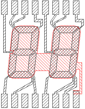
|
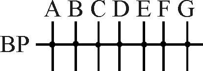
In this example, a single backplane (in red) is shown. This backplane is common to every segment, and the segments are all routed out to a unique pin on the display contact ledge. An individual segment is activated by applying the driving squarewave between the backplane and the individual segment trace. This part will require 14 contacts for the segments and 1 contact for the backplane. The equivalent electrical circuit, in this case trivial, is shown in the drawing above. |
When multiplexing an LCD, appropriate segments are connected together to form groups which are sequentially addressed by means of multiple backplane (sometimes called common plane) electrodes. These groups are organized in a matrix of rows and columns. Typical multiplex drivers generate amplitude varying, time synchronized waveforms, and apply them to the row and column lines of the matrix at a high rate. A full discussion of multiplexing is presented in our App Note Section.
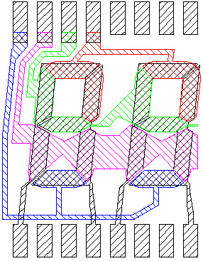
|
In this example, a 4:1 multiplex, the four different colors represent the four backplanes. The equivalent circuit above is more meaningful in this case. As can be seen, BP1 (in red) controls the "A" and "B" segments of the two digits. The "A", "E", and "F" segments all are routed to the edge of the part using a single trace. The "A" segment is therefore turned on by applying the squarewave between BP1 and the first pint on the lower left of the bottom row. By using this multiplexing scheme, the LCD will require only four contacts for the segments, plus an additional four contacts for the backplanes. We have therefore reduced the pin count significantly. |
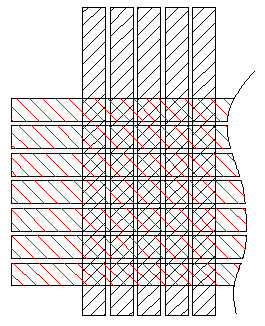
|
This is an example of a pinout for a dot matrix display. Here, every row must be brought to the left edge, and every column must be brought to the top of the part for connection to the PC board. This is usually accomplished by a heat seal or elastomeric connector. See What is a Heat Seal? Elastomer? for an explanation of these connection methods. |
We refer to a display having normally open elements as a positive image display, which has dark activated segments on a light background. Similarly, a display having normally closed elements is referred to as a negative image display, which has light (clear) activated segments on a dark background. The orientation of the front and rear polarizer films on the LCD cell determines whether the display features a positive (crossed polarizers) or a negative (parallel polarizers) image viewing mode.
The contrast ratio and transmission of an LCD is primarily determined by the polarizing efficiency and the percent transmission of the polarizer films. Cell spacing, drive voltage, drive frequency, the wavelength of light, and temperature, also affect the display transmission and contrast ratio.
Contrast or more appropriately put the contrast ratio of a liquid crystal display is the ratio of the light area of a display to the dark area. For a reflective display this is the ratio of the light reflected by the background to the light absorbed by the rear polarizer of any on segment. Stating the contrast ratio is easy, measuring it is not. The contrast ratio will change with the angle and position around the display. As illustrated by the isocontrast plot of a first minima display below, the contrast ratio changes as one tilts away from normal and rotates the display about 360 degrees.
Direct drive displays have excellent contrast over a wide range of viewing directions. Because of the drive scheme used for multiplexed displays, the viewing angle and contrast ratio begin to change more rapidly than direct drive displays, and it becomes important for the user to know how the display will be viewed in the instrument.
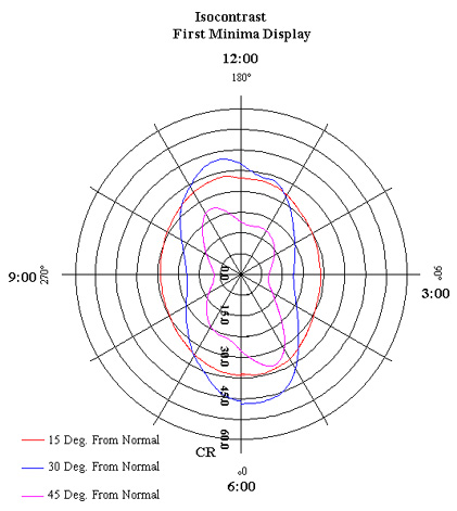
LCD's can be overdriven by a combination of voltage and frequency, which will result in cross talk or "ghosting" Ghosting is the appearance or partial activation of an "off" segment. This condition occurs when high drive voltage and frequency are applied. Since the current is directly proportional to the frequency, there is a voltage-frequency product which must not be exceeded. These values are very dependent on the design and layout of any given part, so proper display design and choice of driving conditions is important. From a design standpoint, the goal is to make the common plane electrode as large as possible to keep the resistance low. It is also very important that all unused segments be connected to the backplane, and not allowed to float.
A full technical discussion of "Ghosting" can be found in our App Notes Section.
Response time is the time it takes for the display to either turn on or turn off. The turn on time is the time it takes, from when an electric field is applied to an active segment, for the contrast to reach 90 percent. The total turn on time can be broken down into two components, the delay time and the rise time, see figure 1 on the bottom of this page. Similarly the turn off time is the time it takes for the contrast to change from fully on to 10 percent. It can also be shown that there is a delay from when the field is removed to the 90 percent point. The total off time is the delay plus the fall time, see fig 2 on the bottom of this page.
For those so inclined, we can also describe the turn on and turn off times mathematically,


Where tr is the total on time, td is the total off time, d is the cell gap, Vapp is Vdd, K is the elastic constants of the liquid crystal mixture and h is the viscosity of the liquid crystal mixture. For a given liquid crystal mixture, the physical parameters are fixed. From the equations above we can see that to decrease the on time we can lower the viscosity, decrease the cell gap, or increase the drive voltage. The cell gap is fixed because of the birefringence of the mixture. This leaves only two variables left, viscosity and drive voltage. As the temperature goes down, the viscosity will go up. To compensate this we will need to either add heat to lower the viscosity or increase the drive voltage.
Increasing the drive voltage has diminishing returns. There is a point where increasing the drive voltage will exceed the input to the LCD driver and where there is minimal gain in the turn on time especially at colder temperatures. Unlike the turn on time which can be decreased by increasing the drive voltage, the off time is purely a physical phenomenon. We cannot drive the display off. We must rely on the surface energies and the molecules falling back into their twisted structure to provide a fast off time. At colder temperatures, the only way to decrease the off time is to decrease the viscosity and we can do that by adding a heater.
The immediate solution for faster displays is to add a heater to the back of the display. Another solution is to develop a fluid with an extremely low viscosity at very low temperatures. LXD is continually looking to push the limits of display performance.
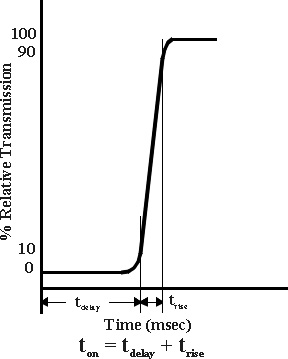
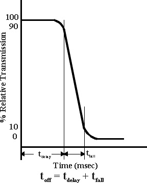
An Icon (or descriptor or annunciator) is a word or special symbol that is driven as a single segment In the sketch below of our standard part #38, the symbols LoBat, AC, DC etc. are turned on as individual segments, so only a single trace needs to be run to a pin for the entire word or picture.
We can create an annunciator from a simple text font, or create a special graphics image using any popular drawing package. We can scan a company logo or picture, or in general make anything into an annunciator that you want. Keep in mind though, that laying out an LCD is similar to laying out a PC board, so that if you want us to put the word "antidisestablishmentarianism" along the top edge of the part as an annunciator, it will block the traces of the other segments from getting to the pins, so it may be a problem.
There are a number of ways to add color to an LCD. Since LCD's do not emit light, the color must come from polarizers, filters, inks, or auxiliary lighting. As is usual, the choice comes down to appearance vs. cost, with cost winning out in most applications.
LXD has approved blue, green and red colored transmissive front polarizers for use in indoor and outdoor applications. For instance, a reflective blue display exhibits medium blue segments on a bluish silver background.
It is also possible for volume custom LCD applications to have a multi-color screened image polarizer. The quantities necessary to justify this approach are extremely high, and the price is somewhat outrageous, however the resulting colors can be worth the anguish.
Colored inks (or colored filters) offer the greatest flexibility for colors in an LCD. The color inks are usually screened on the back (or sometimes the front) of the glass in the desired patterns. For example, a yellow transflector filter is very popular for both positive and negative image very large displays in outdoor message signs. Multiple colors are possible with multiple screen prints. The cost of this approach is the lowest and most adaptable. We recommend backlighting. under all lighting conditions.
|

|
The colors on these displays were applied to the rear of the glass with color inks. In addition, they are negative image displays with a black mask on the front that blocks stray backlight from "bleeding" through.
There are many choices to consider when backlighting an LCD. Once again the choice comes down to appearance vs. cost vs. features. Each approach has its advantages and disadvantages, and no one method is right for all applications. The data below will only give the highlights of each technology with general comments.
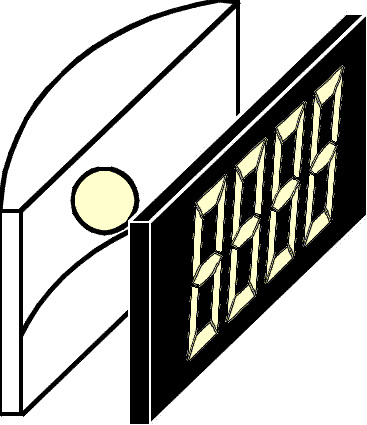
|
Incandescent - Incandescent lights are very bright, however they generate a significant amount of heat, which can cause problems at high temperatures, but may give better display performance at very low temperatures, where they can act as a heater. They can provide very white light, but the color can change with changing supply voltages, and they can be sensitive to shock and vibration. The current consumption is slightly high, but may not be excessive compared to other options, while the price can be very low. |
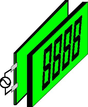
|
Electroluminescence - Electroluminescence is a solid state phenomenon which uses colored phosphors, not heat, to generate light. The main advantages to EL are extremely low current requirements, very low heat generation, uniformity, and thinness. The biggest drawback to an EL panel is that it requires an inverter which draws relatively high current (50-60ma) and takes up board space. The half brightness (half-life?) problem associated with EL needs to be taken into consideration, however by driving the EL panel at lower than rated voltages, the half-brightness problem can be minimized. |
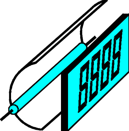
|
Fluorescent -Fluorescent backlights offer very long lifetimes with low heat generation, and low power consumption. Like an EL, they also require an inverter which draws relatively high current. The colors do not change much with a slight decrease in supply voltage, and they withstand shock and vibration very well. Cold weather operation can also be a problem, and should be addressed with the manufacturers. |
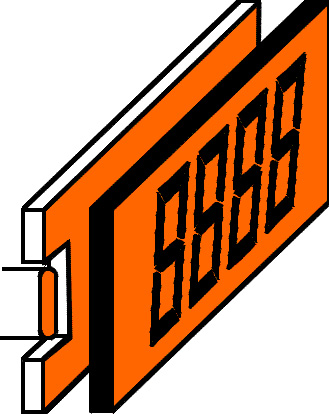
|
LED - The main advantages of LED backlighting are its low cost and long life. Many different colors are also available. The light provided by LED's tends to be rather uneven, however if a suitable light pipe or diffuser is used, the lighting can become uniform. For operation across a wide temperature range, the forward current supplied to the LED's is critical, and must be varied according to the ambient temperature. |
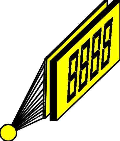
|
Woven Fiber Optics - Fiber optics provides an extremely uniform backlight, without the need for an inverter. The lifetime is dependent on the type of bulb used, with halogen (which generate high heat) or LED sources providing 5000 to 100,000 hours. The bulbs themselves are usually mounted away from the LCD, where they can be easily replaced when necessary. Woven fiber optic panels tend to be somewhat expensive, but the uniformity and brightness are worth the extra cost for some applications. |
The glass used to manufacture LCD's comes overcoated with an ITO (Indium Tin Oxide) layer. We image this ITO layer to form the pattern of digits and annunciators you will eventually see on the finished display. The ITO has a uniform sheet resistance, which is determined at the time the glass is manufactured.
The resistance of the glass is usually in a range between 60 and 180 ohms per square, as measured with a four point probe. A number of customers have asked us, "Ohms per square what?" Ohms per square inch? Ohms per square meter? The answer is Ohms per square anything, or just Ohms per square. The following derivation, which is valid for any very thin film or material, shows how it is measured.
With a four point probe technique, the resistance is measured by passing a fixed known current through two points, and measuring the voltage at two other points, as shown in the drawing below. In practice, the four points are usually colinear, but that is not really a requirement.
The constant current is "injected" on the leftmost pin, and "withdrawn" at the rightmost pin, and the voltage is then measured across the two center pins. If the distance between the pins is equal, "a" in our drawing, the following derivation applies. As will be shown, if the current is fixed to the value of 4.53 ma, the voltage reading on our voltmeter will in fact be equal to the resistance value of the indium.
In the following equations, E is the Electric field and j is the current density.
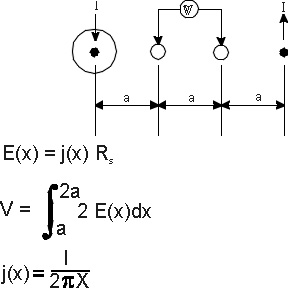
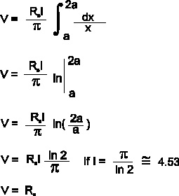
By controlling the input current to the fixed known value of 4.53 ma, the sheet resistance is equal to the voltage across the two test points, and as is seen in the derivation, the units of distance involved have dropped out of the equation.
First Steps in Designing A Custom Display
Design Basics
This introduction is designed to give you a basic working understanding of the design issues you should consider when designing a display product. Feel free to contact LXD to work through your requirements.
Type of Display (Module or Glass Only)
The most fundamental decision to make is if the display will have the drive circuitry attached (module), or not (glass only). There are advantages and disadvantages to each approach.
When purchasing a Custom Module, the basic electronic design work will be done by the module supplier. This obviously saves design time and reduces the manpower needed to bring a product to market. You can benefit from the experience we have gained during our previous designs to shorten the design cycle and deliver an optimized product. The major decisions you need to make are the Interface Type, with standard serial or parallel interfaces being the most common, and the Type of Backlighting desired. The Temperature Range, Viewing Angle, Viewing Mode, and Contrast will need to be considered, but those decisions are common to both approaches.
A Glass Only Design puts the design burden on the end user. You will need to learn a great deal about LCD's in order to complete your design. Fortunately, there is an enormous amount of data available online to help.
The main benefits to buy the LCD glass only are to reduce costs and provide design flexibility. The total cost of the components necessary to build the drive circuitry is less than the cost of a pre-built module. As long as you have space on your existing PC board, you won't have to pay for an extra PC board on which to mount the display. By doing a little homework, your design will work just as well as a module, and will allow the flexibility most designers need to adapt their design to ever-changing demands.
Technology - TN or STN
The type of technology used is determined by the specific performance characteristics of the display you are designing. For a display with a low multiplex rate, i.e. about 8:1 or less, it is possible to use a standard TN cell and still get an acceptable viewing angle and contrast ratio. Above this level, the contrast falls off quickly.
For displays with multiplex rates greater than 8:1, it has been found that increasing the twist angle to 180 to 240 degrees, gives superior results. By using a higher twist angle, one can achieve a larger number of multiplexed lines, with a much higher contrast ratio.
By designing displays with higher multiplex rates, a few problems, which could be tolerated at low multiplex rates, come into play. The first problem is the color. Normal STN cells have a greenish background which is objectionable in some designs. The green color can be corrected. However the correction adds cost to the display. The operating temperature range of the displays also suffers, which may require a heater to overcome.
Viewing Mode - Reflective, Transflective and Transmissive
A Reflective Display has the brightest appearance with the highest contrast ratio possible. However, it will be difficult to read at night or under changing lighting conditions. If your display must be readable under a wide range of lighting conditions, you will generally want a Transflective Display so that it will look very good in the bright sunlight, but will also be backlightable at twilight and at night. A Transmissive Display must always have a working backlight, and is therefore unacceptable in applications where power consumption is a problem.
The tradeoff with a Transflective Display is that it will not look as good as a Reflective Display during the day, and it will not look as good as a Transmissive Display at night. It will however enable you to have an acceptable compromise between the two, and provides a very acceptable appearance. A further discussion of viewing modes can be found in or technical Q & A section under What is Reflective? Transflective?
The display can also be Negative Image or Positive Image. What is Viewing Mode? in our Technical Q & A area discussed these terms.
Viewing Angle (Direction)
The viewing angle of a part is discussed on the What is Viewing Angle page in the Technical Q & A area. In general, the face of the display is divided into quadrants. A display with a 12:00 viewing angle has optimum contrast from above the normal. One with optimum contrast below the normal has a 6:00 viewing angle. Similarly, a display which will be viewed mostly from the left or right should have either a 9:00 or 3:00 optimum viewing angle.
Drive Method
In general, any LCD will have better contrast and viewing angle the lower the mux rate. For parts which are to be viewed under changing lighting conditions, a direct drive part is desirable. Any design which has 14-segment digits will have to be multiplexed to some level, and the mux rate kept as low as possible. This item ties into the next item directly, and the two must be balanced to give the best looking display possible. Direct Drive and Multiplexing are discussed extensively in the Technical Q & A, and Application Notes Sections.
Indoor / Outdoor
In general, the two natural elements that destroy displays are high heat and humidity. The parts of a display which are most sensitive to heat and humidity are the polarizers. Under extreme conditions, the seals which hold the glass together can fail. However, at LXD we have developed materials which effectively eliminate this failure mode. When designing a display for an extremely rugged environment, it is important to make sure that seals will not be a problem. In general then, the environmental considerations comes down to the polarizers.
Displays which will be indoors, or mostly indoors, can use commercial grade polarizers, These polarizers will hold up very well when used in most instrumentation, office and home products, and other applications where the products will be protected from high temperature and humidity.
For harsh environments, a polarizer specifically designed for outdoor and extremely humid conditions should be used. We call these polarizers industrial grade. A wide variety of different outdoor materials is available, with varying contrast, coloration, and efficiency. Because of the many different options, we can supply samples of displays with different polarizers so that you can choose the one which best fits your application.
Color Filters
LXD can add a color decal to the back of the display. This decal can have different colors in different areas so as to give different annunciators different colored backgrounds. This method has the lowest cost, but also gives the dimmest colors.
Screen Print
Similar to the color filters, LXD can screen print different colors onto either the front or rear of the display. Each color can be applied in an intricate pattern, thus giving the same flexibility as the decals but with much brighter colors. This method usually costs more than a color decal, but is the preferred method for most applications.
Color Polarizers
LXD can add a colored polarizer to the front of the display. This method will cause the individual segments to be colored when they are activated, i.e. all segments will be red, green or other color on a silver background. This method will add only slightly to the cost of the display. These colored polarizers are not as efficient as normal polarizers, and the resulting segments do not have the same contrast as a normal black on silver display.
Filters
It is possible to put anti-reflective or anti-glare filters over the front of a display to improve viewability in harsh lighting conditions. These filters are usually bonded directly to the front polarizer of the display.
An anti-glare filter is one that has its front surface either physically or chemically roughened. This surface scatters specular reflections over a wide area. It produces diffuse, bright reflections that will reduce the overall contrast, but can improve the display readability.
A better, but more expensive solution, is to use a high efficiency anti-reflective material. These materials do not scatter the light like the anti-glare materials, but rather re-direct the light waves so that they continue traveling forward instead of reflecting back toward the observer. New anti-reflective materials can reduce the front surface reflections to less than 0.3% or less.
